Decapping a Tamagotchi — Extracting the Die from the Epoxy Blob
by C. Casquatch
This is the first of two posts about a rabbit hole I went down trying to read the code on a Tamagotchi. I wanted to know how the thing actually works at the silicon level, and that meant getting eyes on the die. The chip you’re after isn’t a tidy little package you can desolder and drop into a reader — it’s a chip-on-board (COB) blob, a bare die glued straight to the PCB and drowned in a glob of black epoxy. No package, no pins, no markings, no datasheet. Just a blob.
So before I could read anything, I had to get that epoxy off without wrecking the die underneath. This post is the physical side of the story. The second post covers the other route I tried — going after the data electrically through the board’s test points.
A quick note on naming: this was sold to me as a “Gen 2” Tamagotchi, but the board is modern-production (marked 42800VR5, dated 2024). “Gen 2” describes the gameplay style and shell it imitates, not the chip inside — so I’ll just call it a chip-on-board Tamagotchi and leave the silicon’s exact lineage as an open question.
What we’re looking at
A COB part is about the cheapest way to put a chip on a board. The silicon die is bonded directly to the PCB, wire-bonded to the pads, and then potted under epoxy to protect those hair-thin bond wires. It’s everywhere in cheap consumer electronics for exactly that reason — it’s cheap to make. The downside, if you’re the one trying to reverse engineer it, is that there’s nothing to read from the outside. No part number to look up. The ROM is baked into the silicon itself.
This is the same construction that made the early Tamagotchi ROM dumps such a big deal — there was no easy electrical path in, so people had to get physical.


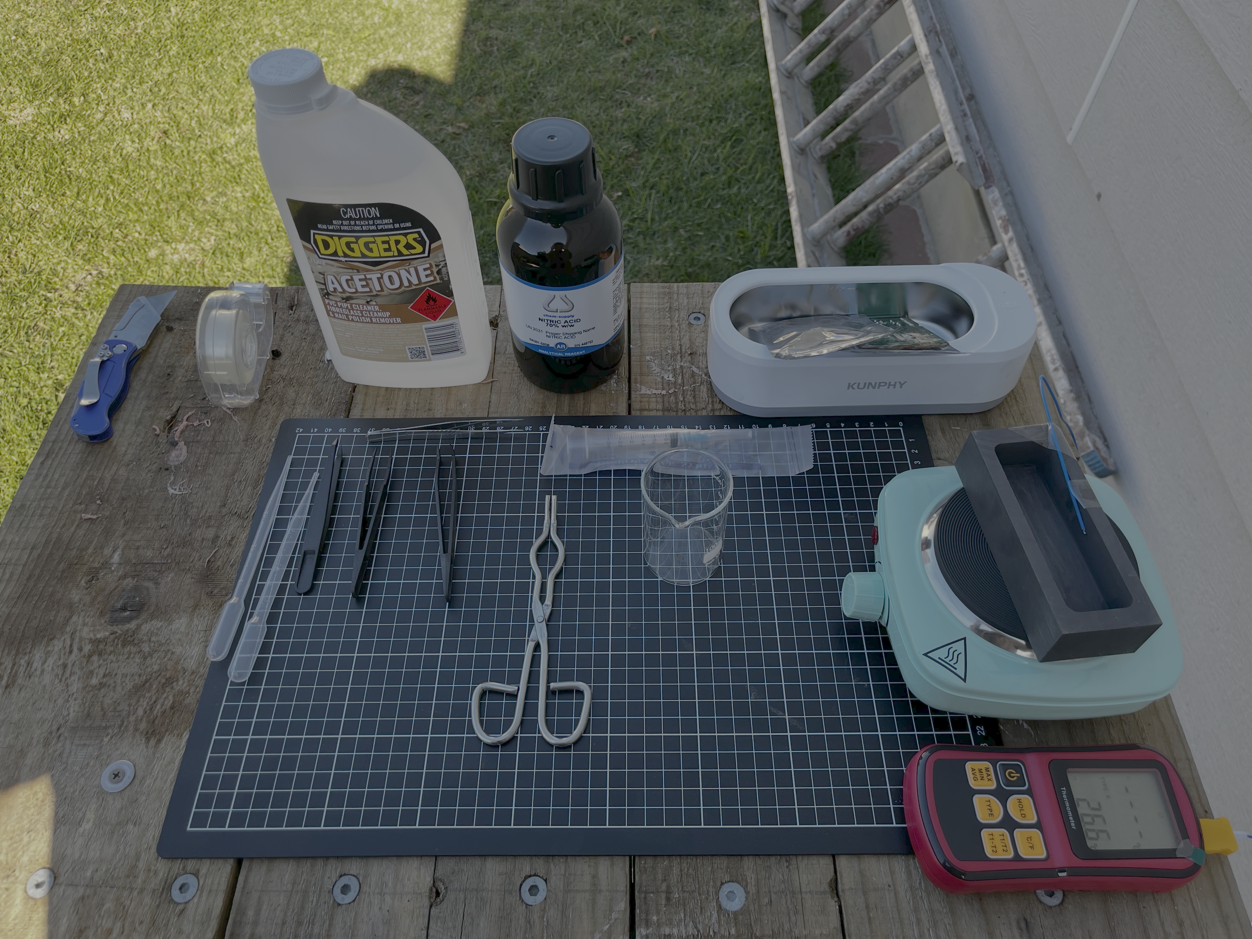
Equipment and PPE
Primary setup outside because of the nitric acid.
Quick word before anyone copies this: the chemistry here is dangerous, not internet-dangerous. Fuming nitric acid does not forgive mistakes. None of this is a how-to — it’s a write-up of what I did. If you don’t already know how to handle these reagents safely, this is not where you learn.
What I used:
- PPE: acid-rated gloves, goggles/face protection, and proper ventilation.
- Small cooktop.
- Beakers (all glass).
- various metal and plastic tweezers of different sizes and pinch types.
- Graphits ingot.
- Thermometer.
- A Dremel for mechanical prep.
- Nitric Acid and Acetone for the chemical decap stage.
- A usb-capable microscope.
- Tongs.
- ultra-sonic cleaner.
- 23 Gauge syringe for nitric acid.
- A pile of junk chips — dead boards I didn’t care about — as practice before I touched anything I wanted to keep.
Step 1 — Mechanical prep (the Dremel stage)
The point of dremelling first is to remove the bulk of the epoxy mechanically so the acid has far less material to chew through. Less acid, less time, less heat, less collateral damage to the surrounding passives.
The whole game here is restraint. You’re trying to thin the blob, not breach it. Go too far and you crack or score the die, or shear the bond wires, and the part is dead before chemistry ever starts. Heat is the other enemy — the epoxy is formulated to survive soldering temps, so grinding generates heat that can cook the die if you lean on it. Short passes, let it cool.
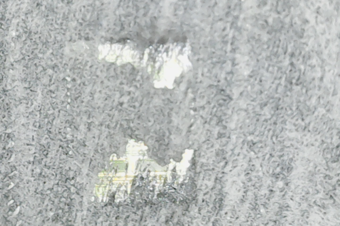
After dremelling some of the tests.

After dremelling the first tamagotchi. As you can see, I was too excited and have already stuffed up - rule of thumb, if you can see part of the die before you’ve even hit it with acid, chances are you’ve scuffed it. This means readability of the die will be poor.

What they look like after being dremelled but before the acid. Scuffed and Stuffed :(
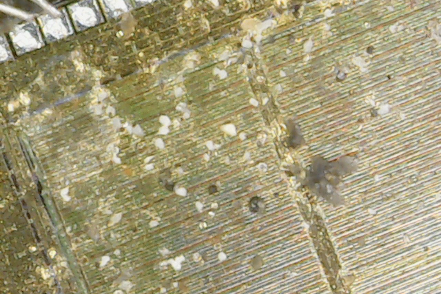
Step 2 — Chemical extraction (burning the epoxy)
This is the stage everyone pictures when they hear “decapping” — the epoxy being chemically eaten away to leave the bare silicon sitting there exposed.


Step 3 — Imaging the die, and another wall
This is the part I am currently unable to get past, besides scuffing my dies.
I got the epoxy off. I exposed the die. On the practice chips and on the Tamagotchi, the chemistry worked — there was bare silicon sitting there to look at. The decap was a partial success.
The microscope I bought was another failure.
What I have right now simply doesn’t resolve enough detail. You can see the die — the rough floor plan, the large structures, the general layout of regions on the silicon. What you can’t do at this magnification is read anything meaningful: no tracing of individual gates, no following the metal layers, nothing close to the resolution you’d need to reconstruct logic or pull a ROM optically. To do that properly you’re into high-magnification optical work or a scanning electron microscope.
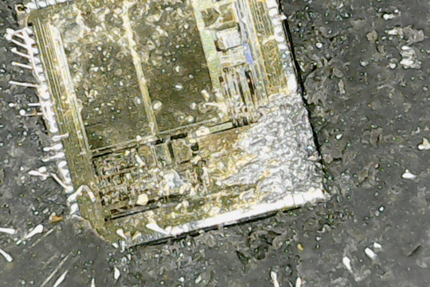
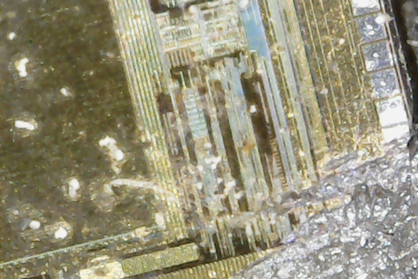
This is as clear as I can get with my current microscope. I could probably find a university or hackerspace that has some access to something more heavy-duty.
Where this goes next
Soldering onto the board’s test points and trying to coax firmware out over a serial line. Spoiler: It went exactly as I thought it would.
Resources
Talks
- 29C3 — Many Tamagotchis Were Harmed in the Making of this Presentation — Natalie Silvanovich (natashenka), CCC 2012. The foundational Tamagotchi reverse-engineering talk; covers why physical access mattered so much on this hardware.
Papers & write-ups
- First Glimpse into the Soul of a Tamagotchi — KwartzLab Makerspace. Early die-level investigation of Tamagotchi hardware.
- Tamagotchi ROM Dump and Reverse Engineering — Hackaday. Covers the full arc from physical access through to ROM extraction.
- Hacking the PIC 18F1320 — bunnie’s blog. Context on reading protected microcontroller memory and why physical access is sometimes the only path in.
- Removing / Decapping an Epoxy Blob — EEVblog forum. Community methods specifically for COB / glob-top removal.
- Learning to Decapsulate Integrated Circuits Using Acid Deposition - My whole post and experiment is thanks to this guy - Juan Carlos Jimenez and his careful instructions on how to do this.
- Chip decapping - more ways - another way to decap chips.
- Chip Decapping on a Budget - Zach Pahle Schmoocon 2020
- Defcon 21 talk - Chip decapping the East (Hard) way
- Bsidse Knoxville 2022 - Travis Goodspeed - An Amateur’s Guide to Microchip Decapsulation Chemistry
- Beginners Guide to IC Reverse Engineering - With a High Likelihood of Survival! - Henny-Brenner Saal
- Decapping ICs with Sulphuric Acid - Hackware v3.7 Lim Jin Gen